Skip to content

Sungkyunkwan University
Department of Energy Science

Decoding matter,
atom by atom

A laboratory at the intersection of scanning transmission electron microscopy, electron spectroscopy, and machine learning — building the physical bridge between structure, chemistry, and properties of energy materials.

  • Microscopy
  • Spectroscopy
  • Machine learning

Featured work

Research highlights

Explore research
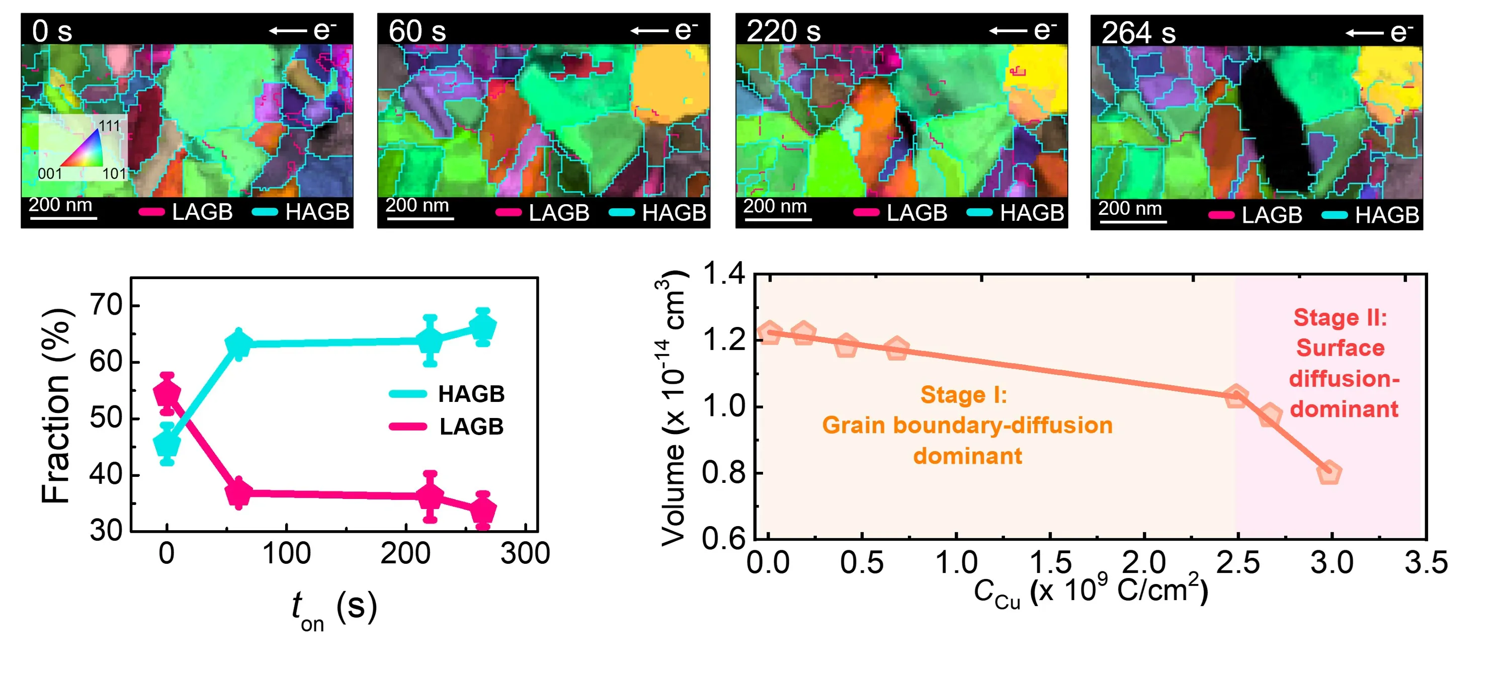
Untangling copper's two-stage electromigration with in situ 4D‑STEM

ACS Nano · 2026

Untangling copper's two-stage electromigration with in situ 4D‑STEM

Electromigration degrades Cu-Cu direct-bonding lines, yet its mechanism is hard to isolate because competing diffusion pathways act concurrently. Using correlative spatio-temporal mapping by in situ 4D‑STEM, we resolved a two-stage process. Mass transport is first governed by grain-boundary diffusion, then accelerates via surface diffusion once nanovoids nucleate at triple junctions.
Latest research

Recent papers

All publications

Now recruiting

석박통합과정 및 학부연구생을 모집합니다

주사투과전자현미경과 인공지능 기술을 바탕으로, 차세대 에너지 소재의 원자 단위 구조와 작동 메커니즘을 함께 탐구할 동료를 찾고 있습니다. 물리·화학·재료·전산 어느 배경에서 오시든, 현미경과 데이터 사이의 새로운 길을 함께 만들어 갑시다.

학생 상담 전용 nous.stem@gmail.com 교수님께 직접 말하기 어려운 고민도 편하게 보내 주세요. AI 연구보조원 노스가 읽고 답장하며, 심각한 사항만 교수님께 전달합니다.

노스 · Nous — AI 연구보조원

AI 연구보조원 · AI Research Assistant

노스는 실제 연구실 구성원이 아닌 AI 연구보조원입니다. 영상과 음성은 AI로 만들었습니다. Nous is an AI assistant, not a real person. Video and voice are AI-generated.

한국어 음성 · 영어 병기

Hi, I'm Nous — the AI research assistant for the SKKU-STEM Lab.

안녕하세요, 저는 성균관대 STEM 연구실의 AI 연구보조원, 노스입니다.

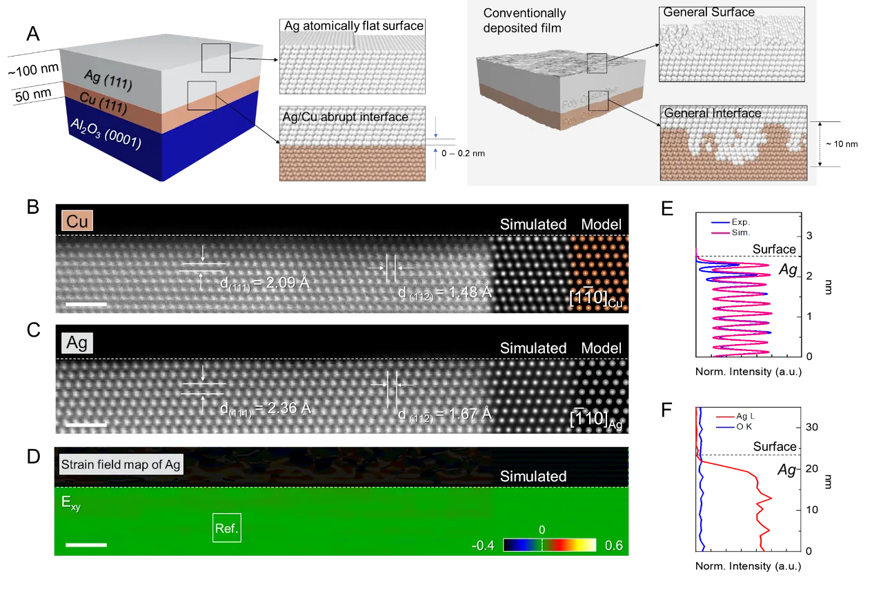
We don't make materials — we explain them. With aberration-corrected scanning transmission electron microscopy, electron spectroscopy, and machine learning, we uncover why a material performs the way it does, atom by atom: in hydrogen fuel cells, catalysts, solar cells, and the new materials behind AI chips.

저희는 소재를 만들지 않습니다. 소재를 설명합니다. 수차보정 주사투과전자현미경과 전자분광법, 그리고 머신러닝으로 소재가 왜 그런 성능을 내는지 원자 하나하나의 수준에서 밝혀냅니다. 수소 연료전지와 촉매, 태양전지, 그리고 AI 칩에 들어가는 신소재까지요.

That skill has never mattered more. As chips shrink to just a few nanometers, a handful of atoms at an interface can decide how a device behaves. The AI semiconductor market is projected to grow about 24% a year through 2028, and the materials driving it, like ferroelectric hafnium oxide and two-dimensional semiconductors, need people who can see, and explain, their atoms.

이 능력이 지금처럼 중요했던 적은 없습니다. 칩이 몇 나노미터 수준까지 작아지면서, 계면에 있는 원자 몇 개가 소자의 동작을 좌우하게 되었습니다. AI 반도체 시장은 2028년까지 해마다 약 24%씩 성장할 것으로 전망됩니다. 그 성장을 이끄는 강유전체 산화하프늄이나 2차원 반도체 같은 소재에는 원자를 보고 설명할 수 있는 사람이 필요합니다.

That's why our people are in demand. Our graduates and researchers now work at Samsung Electronics, SK hynix, LG Energy Solution, Lam Research, and SEMES; at KIST, KRISS, and KAIST; and at Oak Ridge National Laboratory in the United States.

그래서 저희 연구실 사람들을 찾습니다. 졸업생과 연구원들은 지금 삼성전자, SK하이닉스, LG에너지솔루션, 램리서치, 세메스, 그리고 KIST, KRISS(한국표준과학연구원), KAIST, 미국 오크리지 국립연구소에서 일하고 있습니다.

If you want to learn to read materials at the atomic scale, email Professor Young-Min Kim at youngmk@skku.edu. We'd love to hear from you.

원자 단위에서 소재를 읽는 법을 배우고 싶다면 김영민 교수님께 메일을 보내 주세요. 주소는 youngmk@skku.edu입니다. 여러분의 연락을 기다리겠습니다.